Saturday, 29 September 2012

My Alternate Jeenode

The Processor board for my shields arrived this morning and I've finished assembling the parts and tested the GLCD, RFM12B and the SD Card socket.

One of the main reasons behind this PCB is so I can have a driver for the Jeelabs GLCD that is physically smaller than the GLCD PCB and will be easier to mount in an enclosure but now all sorts of ideas are now springing forth!

This is the first time I've used a few SMD components, I'm using the 1206 size because I can just about manage them without too much eye strain.

So far I've tested the GLCD, RFM12B and SD card reader and all seems OK so far.

Eagle Files for PCB are here.

Top view
Bottom View

Screen grab of SD card info sketch.

So far so good, all going to plan.


Monday, 24 September 2012

My own Arduino Shields

Having spent a while playing with the some of the different options available in the world Arduino open hardware and software and discovering a very reasonably priced source of PCB manufacture I've spent more time designing the hardware than I have the software side of things, I have a few plans for final applications but keep getting side tracked by new ideas of what to do with the hardware.

Anyway my latest idea was to create my own PCB to plug on the back of the GLCD hardware from Jeelabs, one that was a similar size and shape to the GLCD.

Whilst doing that I was also thinking about producing a CAN interface PCB for the new layout that could be sandwiched between the processor PCB and the GLCD PCB and I wanted a method to allow me to validate the PCBs within a 3D environment.  After a quick Google I found that there were scripts written which would allow the PCB in Ealge (Circuit layout and PCB design software) to be exported in a format that would allow Google SketchUp (Free 3D design software) to import the PCB with holes, vias, silk text and tracks, this made it a lot easier to visualise the PCBs and hopefully spot any errors prior to ordering the PCBs.

Within Google  SketchUp  there is access to the 3D Warehouse where people generate models for all sorts of things and make them available for other people to use and there are quite a few electronic components in there, including Arduino boards.

I also had to model a few parts myself, like the Jeelabs GLCD and PCB assembly, Sparkfun's Basic FDTI board.  If you want to use the models just search for GLCD in the 3D warehouse and you should find them.

If the Eagle export setup is configured correctly and the models are available in the correct folder the export will also include the components on the PCB as well.

The the setup tutorial and link to the software download can be found here.

Here are some of the exports I made from Eagle, these have also been rendered by a  SketchUp  plugin called Maxwell.
The three PCBs exploded view and rendered

CAN Interface PCB with most of the components

GLCD board plugged into the processor board

All three stacked together

Wednesday, 29 August 2012

All in one Prototyping PCB assembly

The assembly of the PCBs finally got started over the weekend and so far I'm pretty pleased with them, I've spotted a couple of minor issues so far but nothing that can't be fixed with a sharp knife some wire and a soldering iron.

Eagle files can be found here, they are version 2 with the power supply fixed and an added higher power 5V regulator.

So far I've only tried the ATMega 328p and it's peripherals, the ATtiny84 can wait until next weekend.


Firstly I added all the resistors, they need to be quite small resistor, physically that is, as I only used a 5mm lead pitch package.  I then added the voltage regulators so I could check that power appeared correctly at all the places it should do and at the right level.

This is where I spotted my first error, originally I'd planned to feed the 3.3V regulator from the output of the 5V regulator but then for some strange reason I changed it so both regulator inputs were tied together, unfortunately this meant that when the USB to serial (FTDI) was connected it wouldn't supply the 3.3V regulator and therefore the processor wouldn't be powered.

I cut the track from the supply to the input of the 3.3V regulator and wired it to the output of the 5V regulator. this meant that the FTDI 5V was fed into the 3.3V regulator and supplied the processor.


One of the first things I tried when I got the boards was to plug in the GLCD from Jeelabs as I use this quite a lot, luckily it fit perfectly and it even works.


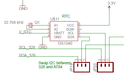
Today the RTC chip arrived with a clock crystal and was soldered in place, not as difficult as I thought it would be.
Added a CR2032, loaded the RTC sketch and used my RTC time setting app for the PC to set the time and it worked fine.

So far so good.....

Saturday, 11 August 2012

328p / ATtiny84/85 Programming Adapter PCB

The Multi programming add-on PCB for my USBTiny programmer arrived today.

Just built one to test.

The ZIF socket came from HongKong via Ebay.

Just connect it to the ISP programming cable from the programmer, make sure the programmer can supply 5V and then you ca program your own boot loaders or sketches and use the Arduino IDE to program the ATtiny84s.

If you want the schematic or PCB files (Eagle CAD) let me know in the comments, also I have some surplus PCBs to requirements so if you want one then I may let some go a cost plus postage and packaging.

Link to the Eagle sch and brd files here.


Friday, 3 August 2012

328 All in one Schematic

Here's the schematic for the PCB on the earlier post. PDF of schematic


The schematic is laid out in sections: -

Dual power supply
Various power supply options
RTC connected to 328p or ATtiny84
Two I2C ports from 328p (should work with I2C Jeeplugs)
Prototyping area


As usual feedback is welcomed.


Wednesday, 1 August 2012

All in one Arduino Prototyping solution

I've been interested in the open HW/SW platform "Arduino" for some time now, it has re-ignited my interest in electronics, which hasn't been at the forefront of my hobbies for some time.
My main interest lay in the area of computers and software but with the discovery of the Arduino platform I was able to merge the two together.

I've bought a few pieces of hardware from various sources and  had a dabble at making my own hardware (mainly copied  based from what others have already done).

Anyway I decided I needed a project of my own to get my teeth into, I wanted to learn how to use the Eagle schematic capture and PCB layout software and after discovering Seeedstudio and their very keenly priced PCB manufacture, I decided to make a general purpose PCB that would allow me to tinker with both the ATMega 328 and the ATtiny84 processors along with various extras.

This board isn't aimed at a final solution but more an electronics breadboard much like the old Tandy electronics kits I used to play with many, many years ago.

Basic Features

  • Independent ATMega328p and ATtiny84 on the board
  • Each having its own RFM12B and ISP programming connector.
  • Twin power supplies, 5V and 3.3V with the option of using a CR2032.
  • A series resistor option for measuring supply current, jumpered out if not required.
  • A prototyping area.
  • A 4 port layout like the Jeenode (so I can plug in my GLCD).
  • A RTC (DS1307 3.3V)
  • Two I2C ports connected to the 328P with 5V and 3.3V (should work with Jeelabs plugs)
  • FTDI connector (328p)
I've not ordered the PCBs yet as I'm fine tuning the board still but should be doing it in the next week or so.

PCB
Comments welcome.

Tuesday, 24 July 2012

ATtiny board blinking

Well I got around to adding some components to the PCB, and found a couple more "improvemments" that can be made.  They're mainly around the package size of the RF12B transceiver, even though it was pointed out in other blogs I fell into the same trap, I moved the battery connections down a bit to clear the RF12B but forgot about the top so that the lower leg of R3 has a hard clash with the top of the RF12B PCB.

I've now gone into the symbol for the RF12B and added a couple of mm to the package outline and improved the PCB layout by rotating R3 90 degrees to clear the RF12B PCB. Ready for the next batch, if I ever need any more!

I programmed a blink sketch into an '84 and plugged into a PCB, added an LED between PB0 and VCC GND and it actually worked.

Next job is to add the RF12B and start to read temperatures from the DS18B20(s) and get them transmitting.

I've also ordered some 2xAAA battery holders with switches from ebay so I can easily power the boards.

If all goes well I will even have a go at logging data to an SD card, another ebay purchase.

Testing LoRA transmitters and receivers

I've wanted to have a play with 868MHz LoRA transmitters for some time now but never got around to it until,  a while ago, I did an hard...

Popular Posts